- Welcome to LEC Forum.

Recent posts
#51
Modbus / Modbus Device Limits
Last post by Dave Loucks - February 24, 2015, 07:40:51 AMAs many know, and EIA-485 network can support 32 devices (31 slave devices + 1 master) over 4000 feet (1219 m) as long as you set the bit rate to no more than 100 kbps (higher bit rates limit distances allowed). Also, in the original Modbus specification the highest usable Modbus address is 246 (0 and 247-255 have special purposes). The mMINT adheres to this standard.
Now for the mMINT, an additional consideration might be the INCOM network limits, but since INCOM supports up to 4095 unique addresses and up to 10000 feet (3048 m) of twisted pair, the real limitation is the 246 uniquely addressable stations on the Modbus network.
Therefore for mMINT systems you can only have 246 unique devices on the INCOM network since you need one Modbus address for each INCOM device connected downstream of a mMINT. So while you can have 4095 unique INCOM address 001-FFF on the INCOM side, that isn't any use since you can't have more than 246 unique Modbus addresses.
Here's a diagram:
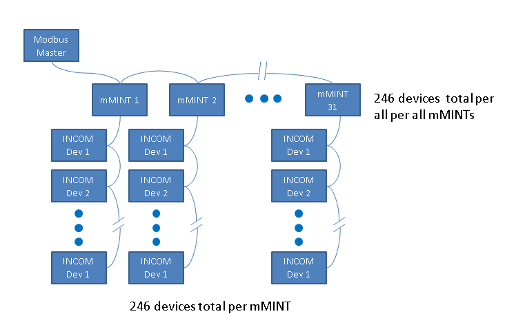
This 246 per leg and 246 total might be confusing, but it just is to say you cannot have more than 246 devices on any single mMINT, but you can also not have more than 246 total Modbus devices on all mMINTs that might be connected to a single Modbus network.
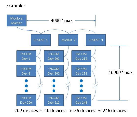
To show how these limits work, here's an example of where you can load up a single mMINT, but could also put several more devices on two other mMINTs where all three mMINTs are on the same Modbus network to bring the total up to 246 devices.
If this isn't enough devices, you get another 246 on a second port on the same Modbus master:
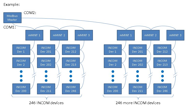
Using this technique you can build arbitrarily large systems -- recognizing that for practical systems, the desired throughput/update time will limit the number of devices.
Depending on how much data you want to collect and how fast you want to collect it will establish a practical upper limit on the number of devices per COM port.
Now for the mMINT, an additional consideration might be the INCOM network limits, but since INCOM supports up to 4095 unique addresses and up to 10000 feet (3048 m) of twisted pair, the real limitation is the 246 uniquely addressable stations on the Modbus network.
Therefore for mMINT systems you can only have 246 unique devices on the INCOM network since you need one Modbus address for each INCOM device connected downstream of a mMINT. So while you can have 4095 unique INCOM address 001-FFF on the INCOM side, that isn't any use since you can't have more than 246 unique Modbus addresses.
Here's a diagram:
This 246 per leg and 246 total might be confusing, but it just is to say you cannot have more than 246 devices on any single mMINT, but you can also not have more than 246 total Modbus devices on all mMINTs that might be connected to a single Modbus network.
To show how these limits work, here's an example of where you can load up a single mMINT, but could also put several more devices on two other mMINTs where all three mMINTs are on the same Modbus network to bring the total up to 246 devices.
If this isn't enough devices, you get another 246 on a second port on the same Modbus master:
Using this technique you can build arbitrarily large systems -- recognizing that for practical systems, the desired throughput/update time will limit the number of devices.
Depending on how much data you want to collect and how fast you want to collect it will establish a practical upper limit on the number of devices per COM port.
#52
3-Phase Power / Real and Reactive Power Analys...
Last post by Dave Loucks - February 19, 2015, 02:46:03 PMLots of good material on the web, but I've sometimes found it confusing to understand why reactive power flow to an inductor is considered "positive", but at the same time you hear that the phase angle of inductor current is lagging (which to my ear sounds "negative"). For capacitors this is reversed (e.g. negative reactive power flow for leading current). Anyway, I thought I'd outline a quick overview of how all this fits together.
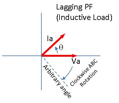
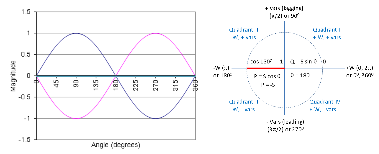
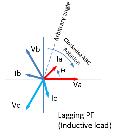
We begin with a diagram that might be familiar to many. It shows real power flow on the x-axis and reactive power flow on the y-axis. Since both forward and reverse (positive and negative) real and reactive power flow is possible, there are four categories (+W/+vars, +W/-vars, -W/+vars, -W/-vars) that the diagram places in separate quadrants. I've shown it with ABC clockwise rotation (meaning that increasing angles are increasingly "lagging" which is explained below).
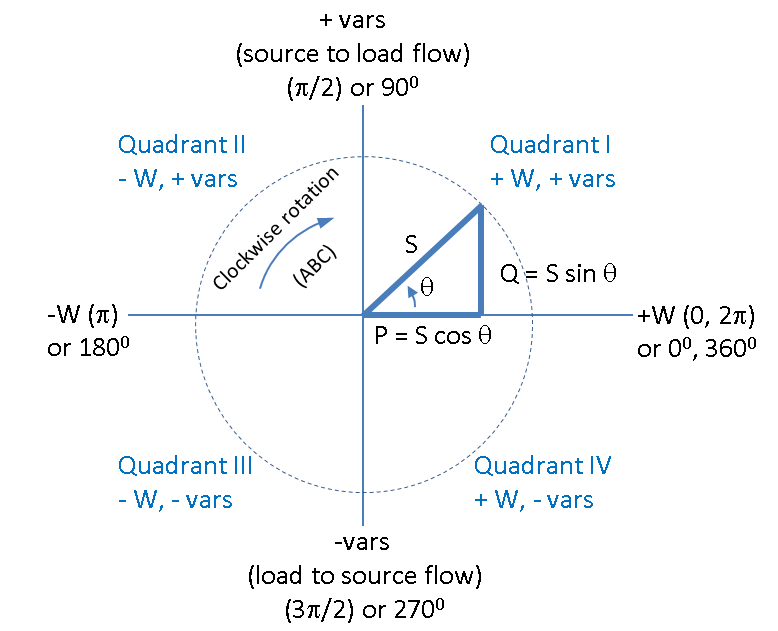
The circle shows the line etched by a constant value of S at different values of
The exact same value of S (VA or apparent power) can result in a variety of different P (real) and Q (reactive) values just by changing the phase angle!
So what is the phase angle and how do you calculate it?
Let's say you just define the voltage reference right now to be 00 and you measure your current to be
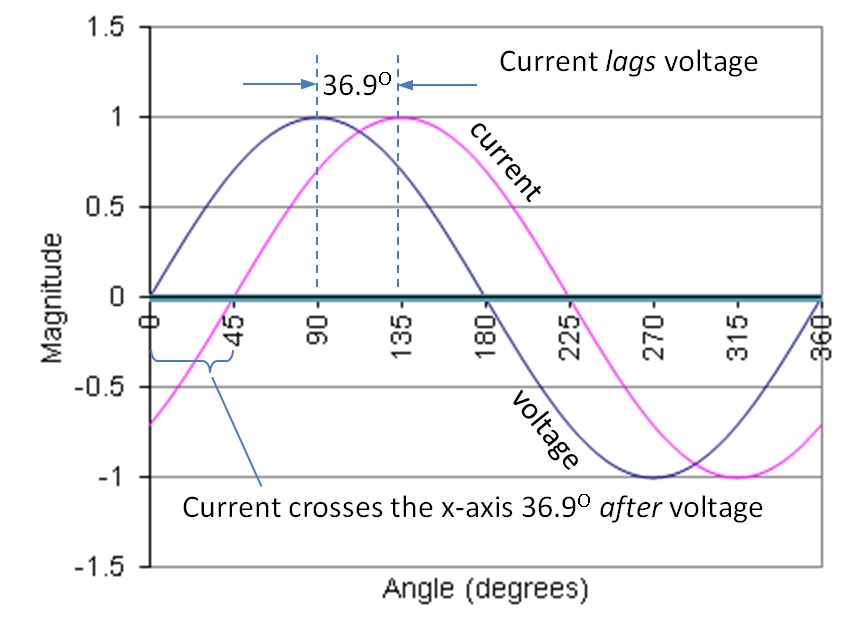
Here's a diagram of system with where the current is lagging the voltage by 36.9 deg.
Here's where it gets somewhat tricky... the current is delayed by 36.9 degrees, which might sound like a "negative" angle, but you can see from the phasor diagram as shown that it actually is a more positive phase angle.
sin (36.90) = 0.6
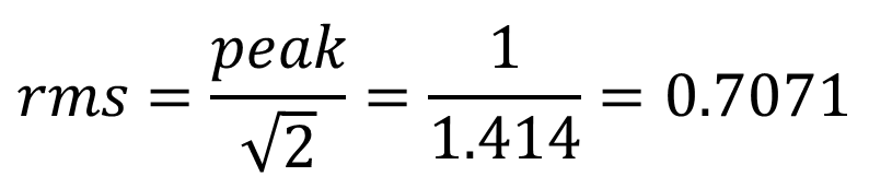
By the way, in these waveforms the peak voltage and current were both 1. When we calculate power (whether real or reactive), we use root mean square versions of the signals. Since we have a two nice sine waves the rms value can be calculated easily from the peak:
In a single phase system:
Plugging and chugging:


Note that sin (-36.90) = - sin (+36.90). This means that moving the phase of the current either ahead or behind the voltage causes leading (positive) var production or lagging (negative) var consumption, respectively.
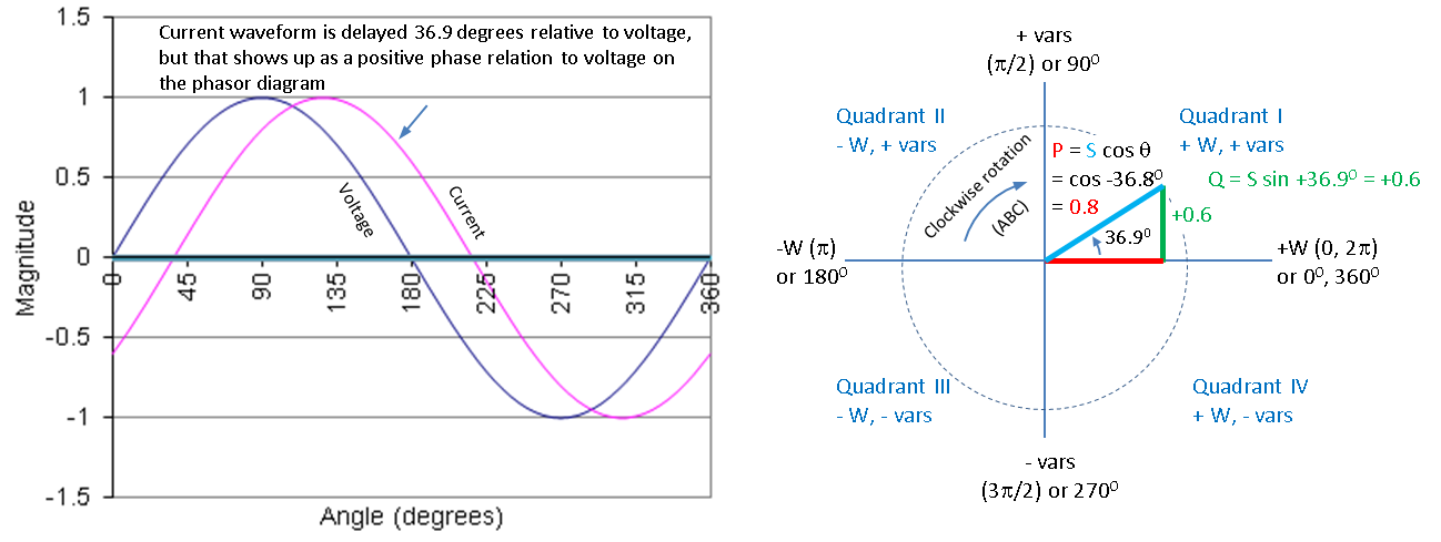
That is not the case for the real power (cosine). Since cos(-36.90) = cos(+36.90) = 0.8 this tells you that changing PF over this range doesn't affect real power flow over this small range.
.png)
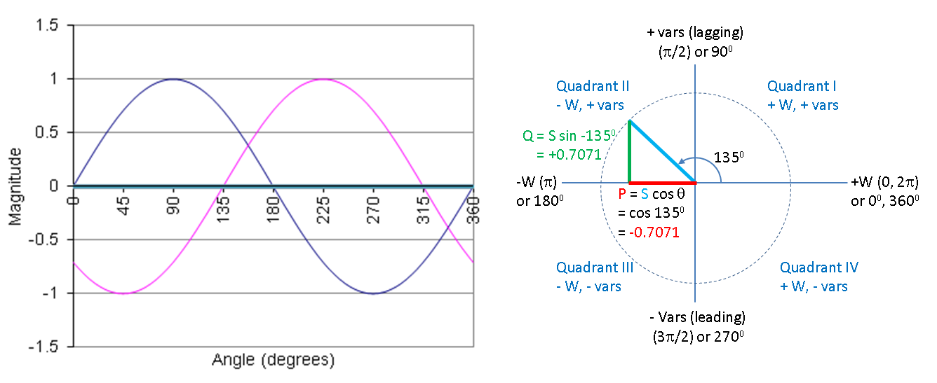
The waveform and phasor diagrams show how the same value of S (in these cases it is assume to be 1) can result in very different values of P (real) or Q (reactive) power.
The phase angle of the current relative to the voltage would need to increase to more than 90 degrees (but less than 270 degrees) in order for the the sign of the real (W or P) term to turn negative. This makes sense since consider a signal exactly 180 degrees out of phase. 180 degree out of phase current would look like this:
It is by convention among power systems engineers that capacitive circuits "produce" vars and have leading PF and inductive circuits "consume" vars and have lagging PF. Here's an example where the current leads the voltage by 135 degrees resulting in negative real power, but positive reactive power.
In the scheme of things this is totally arbitrary because ideal versions of both components never "keep" the vars. They store energy during a portion of the half cycle and then return it the next.
So why do people talk about capacitors "producing vars"?
It is just convention to say that the reactive power is "consumed" when it is positive and "generated" when it is negative. From the diagrams above, negative vars occur when you have leading power factor.
Maybe then someone asks "why do capacitor circuits result in leading phase angles and inductors result in lagging phase angles?"
Let's start with looking at a leading PF circuit.
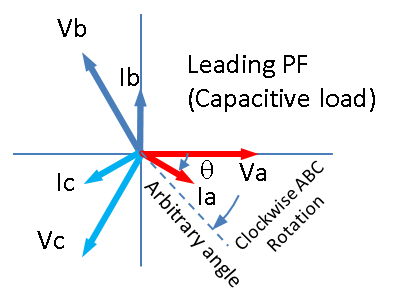
This is a 3-phase diagram, but it works for 1-phase (just remove the B and C phases). The way I look at it is to realize that the phasors are rotating in time. At the instant this "snapshot" was taken, the Va phase was exactly aligned with the x-axis (00), but that is totally arbitrary. What is important is the angle between that voltage and its corresponding phase current. While we said at this instant the voltage was measured and/or defined to be at 0 degrees, a millisecond later it may not be.
As these phasors rotate (I'll assume clock-wise for ABC rotation, meaning first A, the B, then C cross the 00 axis as it rotates...), the Ia phase will always cross any arbitrary angle before the Va phasor "gets there".
Since current "gets there" before the voltage we say the current is leading the voltage.
Here's the "why" that this happens. Capacitors look like short circuits when discharged. For a moment in time after you apply a non-zero charging current, the voltage is 0 until it begins to charge up. A voltage of 0, by definition, is a short-circuit. In an ideal short circuit, infinite current flows but there is no voltage drop. Now, in the physical world that isn't the case, but you will see current flowing in a capacitor before the voltage changes. How fast that happens depends on the size of the capacitor and the voltage applied. If you have current flowing before voltage changes, then that is another way of saying current changes precede (or lead) voltage changes -- or more simply, current leads the voltage. This can also be described by looking at the mathematical relationship between current and voltage in a capacitor. Danger Will Robinson - Differential Equations ahead :
:
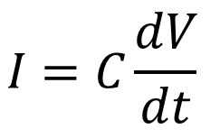 What this says is that for voltage to change instantaneously (dt = 0) you would have to apply infinite current. Guess that isn't going to happen! So for capacitors, any nominal current will result in a delayed voltage change, or in the vernacular of speaking about current in relation to the voltage we say the current leads the voltage.
If the phase angle was reversed, the voltage would cross any arbitrary angle before the current and we'd say the current lagged the voltage. Here's that phasor diagram:
This is known to be an inductive circuit since with inductors no current flows immediately after a voltage change is applied across the inductor. Mathematically we write:
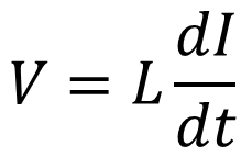
According to this equation, for the current in an inductor to change instantaneously (dt = 0) you would have to apply infinite voltage. That ain't gonna happen either, so the result is that current can't change instantaneously with a voltage change and we say the current lags the voltage.
Armed with this fabulous knowledge, we can then attack the problem using our standard trig equations that show how to solve for unknown values of a right triangle.
If, for example, you know its hypotenuse (S or VA or apparent power) and you have been given either one other side (kW) or the angle (PF) you're good to go.
You can derive everything else using these equations:
W = Wh / h
Q = varh / h
S2 = W2 + Q2
cos-1(W/S) =
W = S cos
cos
sin-1(Q/S) =
Q = S sin
sin
tan
To help visualize these phase angles, I've attached two Excel spreadsheets that can be used to create a voltage waveform, then superimpose on the same graph the current waveform. I went ahead and included the ability to add harmonic currents (which is a topic for a future discussion).
We begin with a diagram that might be familiar to many. It shows real power flow on the x-axis and reactive power flow on the y-axis. Since both forward and reverse (positive and negative) real and reactive power flow is possible, there are four categories (+W/+vars, +W/-vars, -W/+vars, -W/-vars) that the diagram places in separate quadrants. I've shown it with ABC clockwise rotation (meaning that increasing angles are increasingly "lagging" which is explained below).
The circle shows the line etched by a constant value of S at different values of
θ
(0 to 360 degrees).The exact same value of S (VA or apparent power) can result in a variety of different P (real) and Q (reactive) values just by changing the phase angle!
So what is the phase angle and how do you calculate it?
Let's say you just define the voltage reference right now to be 00 and you measure your current to be
θ
degrees away from that axis. Depending on which way the angle points (above the x-axis or below) determines whether the power factor is lagging (consuming vars) or leading (producing vars), respectively.Here's a diagram of system with where the current is lagging the voltage by 36.9 deg.
Here's where it gets somewhat tricky... the current is delayed by 36.9 degrees, which might sound like a "negative" angle, but you can see from the phasor diagram as shown that it actually is a more positive phase angle.
sin (36.90) = 0.6
By the way, in these waveforms the peak voltage and current were both 1. When we calculate power (whether real or reactive), we use root mean square versions of the signals. Since we have a two nice sine waves the rms value can be calculated easily from the peak:
In a single phase system:
- S = V * A
- P = S * cos(θ) = V * A * cos(θ)
- Q = S * sin(θ) = V * A * sin(θ)
Plugging and chugging:
Note that sin (-36.90) = - sin (+36.90). This means that moving the phase of the current either ahead or behind the voltage causes leading (positive) var production or lagging (negative) var consumption, respectively.
That is not the case for the real power (cosine). Since cos(-36.90) = cos(+36.90) = 0.8 this tells you that changing PF over this range doesn't affect real power flow over this small range.
The waveform and phasor diagrams show how the same value of S (in these cases it is assume to be 1) can result in very different values of P (real) or Q (reactive) power.
The phase angle of the current relative to the voltage would need to increase to more than 90 degrees (but less than 270 degrees) in order for the the sign of the real (W or P) term to turn negative. This makes sense since consider a signal exactly 180 degrees out of phase. 180 degree out of phase current would look like this:
It is by convention among power systems engineers that capacitive circuits "produce" vars and have leading PF and inductive circuits "consume" vars and have lagging PF. Here's an example where the current leads the voltage by 135 degrees resulting in negative real power, but positive reactive power.
In the scheme of things this is totally arbitrary because ideal versions of both components never "keep" the vars. They store energy during a portion of the half cycle and then return it the next.
So why do people talk about capacitors "producing vars"?
It is just convention to say that the reactive power is "consumed" when it is positive and "generated" when it is negative. From the diagrams above, negative vars occur when you have leading power factor.
Maybe then someone asks "why do capacitor circuits result in leading phase angles and inductors result in lagging phase angles?"
Let's start with looking at a leading PF circuit.
This is a 3-phase diagram, but it works for 1-phase (just remove the B and C phases). The way I look at it is to realize that the phasors are rotating in time. At the instant this "snapshot" was taken, the Va phase was exactly aligned with the x-axis (00), but that is totally arbitrary. What is important is the angle between that voltage and its corresponding phase current. While we said at this instant the voltage was measured and/or defined to be at 0 degrees, a millisecond later it may not be.
As these phasors rotate (I'll assume clock-wise for ABC rotation, meaning first A, the B, then C cross the 00 axis as it rotates...), the Ia phase will always cross any arbitrary angle before the Va phasor "gets there".
Since current "gets there" before the voltage we say the current is leading the voltage.
Here's the "why" that this happens. Capacitors look like short circuits when discharged. For a moment in time after you apply a non-zero charging current, the voltage is 0 until it begins to charge up. A voltage of 0, by definition, is a short-circuit. In an ideal short circuit, infinite current flows but there is no voltage drop. Now, in the physical world that isn't the case, but you will see current flowing in a capacitor before the voltage changes. How fast that happens depends on the size of the capacitor and the voltage applied. If you have current flowing before voltage changes, then that is another way of saying current changes precede (or lead) voltage changes -- or more simply, current leads the voltage. This can also be described by looking at the mathematical relationship between current and voltage in a capacitor. Danger Will Robinson - Differential Equations ahead
:If the phase angle was reversed, the voltage would cross any arbitrary angle before the current and we'd say the current lagged the voltage. Here's that phasor diagram:
This is known to be an inductive circuit since with inductors no current flows immediately after a voltage change is applied across the inductor. Mathematically we write:
According to this equation, for the current in an inductor to change instantaneously (dt = 0) you would have to apply infinite voltage. That ain't gonna happen either, so the result is that current can't change instantaneously with a voltage change and we say the current lags the voltage.
Armed with this fabulous knowledge, we can then attack the problem using our standard trig equations that show how to solve for unknown values of a right triangle.
If, for example, you know its hypotenuse (S or VA or apparent power) and you have been given either one other side (kW) or the angle (PF) you're good to go.
You can derive everything else using these equations:
W = Wh / h
Q = varh / h
S2 = W2 + Q2
cos-1(W/S) =
θ
W = S cos
θ
cos
θ
= W/Ssin-1(Q/S) =
θ
Q = S sin
θ
sin
θ
= Q/Stan
θ
= sin θ
/ cos θ
= (Q/S)/(W/S) = Q/WTo help visualize these phase angles, I've attached two Excel spreadsheets that can be used to create a voltage waveform, then superimpose on the same graph the current waveform. I went ahead and included the ability to add harmonic currents (which is a topic for a future discussion).
- 1-phase_harmonics.xls
Allows entering the phase shift as power factor. The spreadsheet will perform the math to shift the current waveform. - 1-phase_harmonics_Phase_shift.xls
Allows entering the phase shift in degrees. - X over R2.xls
Converts PF to X/R and reverse. Calculates Z, %Z, X/R, R, X and L for a given voltage, desired and current. Useful when creating a simulation and you want to choose an R and X to limit current to a particular short circuit value at a particular X/R ratio. - phase_angle_diagram_V1_V2.xls
Allows entering the phase shift in degrees and seeing corresponding changes to real, reactive and apparent power.
#53
Modbus / Primary and Secondary Cause Re...
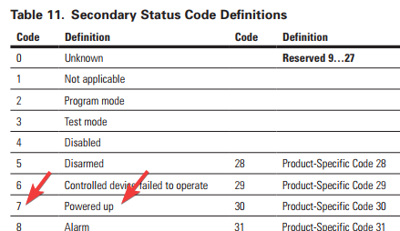
Last post by Dave Loucks - February 02, 2015, 12:12:31 PMHere's how to read and decode these registers:
Here's how to convert that big 32-bit number into three numbers that correspond to the codes you'll see in Tables 10 (Primary Status Code Definitions), 11 (Secondary Status Code Definitions) and 12 (Cause-of-Status Code Definitions)
Example:
Read two register pair 404609-404610 -> returns 32-bit value 66055
66055/65536 = 1.004013... -> Table 12 = 1 (Normal Operating Mode)
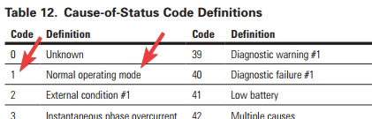
66055 - (1*65536) = 519
519/256 = 2.0273... -> Table 10 = 2 (Closed)
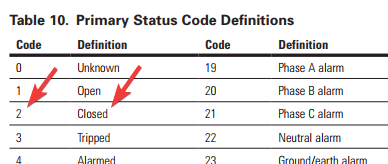
519 - (2*256) = 7 -> Table 11 = 7 (Powered up)
- You must read both registers (404609 and 404610 [floating point] or 406145 and 406146 [integer]) in one Modbus message.
You can't just read one register at a time. You'll get an error! You can read more than 2 registers at a time, as long as the block of registers you read ends by reading a complete register (if it is a 2-register pair, you must read both... a 4-register value, you must read all 4, etc.).
To retrieve the register pair as floating point, depending on your system you may only specify the starting register and the type (float). After all, a single precision IEEE floating point value uses 32-bits so that means you need 2 registers.
Your system may automatically know that and read two Modbus registers (example Tridium JACE 8000 running Niagara 4) when you specify you are reading a floating point register.
For reading these status values from the integer registers (406145-406416) some systems, may automatically retrieve both registers if you specify that you wish to read a "long" integer (example Tridium JACE 8000 running Niagara 4).
For other systems you may need to specify that you wish to read two 16-bit registers and you will manipulate them as separate values.
In particular, in the mMINT Modbus memory map notice that the next higher registers past these status registers contain currents and they are also 2-register pairs (since both integer and floating point values are 32-bit values, stored in 2 16-bit registers). If you decide to include those registers in the same read message, you must set your length to read only complete pairs of registers for a complete register. If you were to end your read to only read the first half of a register, you'll get an error.
- Those two registers hold one large number that must be subdivided into 3 parts!
Appendix A, #12 on page 15 in the IL tables 10, 11 and 12 show how to interpret the data for those three parts
Here's how to convert that big 32-bit number into three numbers that correspond to the codes you'll see in Tables 10 (Primary Status Code Definitions), 11 (Secondary Status Code Definitions) and 12 (Cause-of-Status Code Definitions)
- Divide the number returned by 216 (65536)
The quotient is the code for Table 12 (Cause-of-Status Code) - Now subtract from this number (quotient * 65536) to give the combined Table 10 and 11
- Divide the combined Table 10/11 value by 256
The quotient is Table 10.
Now subtract this new quotient from the Table 10/11 value to give the Table 11 value
Example:
Read two register pair 404609-404610 -> returns 32-bit value 66055
66055/65536 = 1.004013... -> Table 12 = 1 (Normal Operating Mode)
66055 - (1*65536) = 519
519/256 = 2.0273... -> Table 10 = 2 (Closed)
519 - (2*256) = 7 -> Table 11 = 7 (Powered up)
#54
Numa Logic Programmable Controllers / Re: PC 700, 900, 1100, 1200 Pr...
Last post by Dave Loucks - January 18, 2015, 10:08:09 AMNote: During the instructions below, you will see times where function keys must be pressed. If after pressing a function key it only flashes (and no other action seems to take place), you must confirm it by next pressing the <Enter> or you can cancel it by pressing <backspace>. Pressing <Esc> returns you to the main menu.
Save Program to Disk
Save Program to Disk
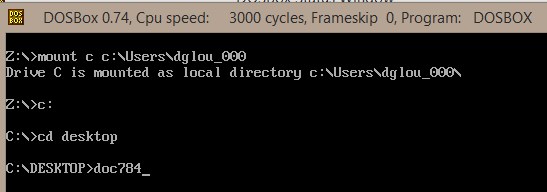
- (Shown using DOSBox emulation on a Windows 8.1 machine) Using C: and CD... commands in DOS, navigate to the directory where you have stored DOC784.exe. Type doc784 from the DOS prompt and press Enter.
You will be brought to the main menu.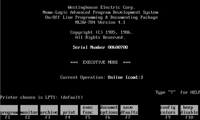
To bring up the list of keyboard shortcuts, you can press ?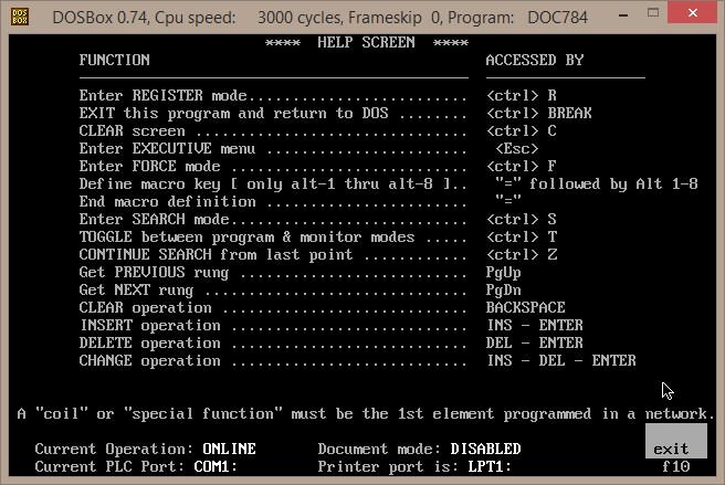
- Unless you are connected with an actual Westinghouse programmable controller (700, 900, 1100, 1200, 1250), it will be better to switch the software into offline mode. Press the F5 Executive Functions key, then select the F2 Online/Offline key.
Press the F2 Offline key.
Using the keyboard arrow keys, select the controller type and memory. Note: the PC1200/1250 choice is not shown. As long as the 1200 program is 8K (16-bit) words or less and 32 analog I/O or less, you can chose the PC700 with "All SFs (special functions)".
If you know the actual target controller, chose F1 default special functions. Changing these settings doesn't affect the program in the offline machine, rather it only prevents you from selecting a special function that is not available in the target controller. If you are only editing an existing program, selecting F3 configure all special functions will insure that the program stored on disk (if you have a disk) will not be rejected as having "unsupported special functions". For this demonstration, assume F1 default SFs was chosen. Select F1 yes to continue, then press enter. Press <Esc> (or press F10 three times) to return to the main menu.
Note:
Besides special functions being different in different processors, each processor supported different amounts of I/O and internal registers. The PC-1100 programmable controller was available in four operational memory sizes: 512, 1536, 2560 and 3584 words of RAM. Each PC-1100 memory configuration supported 64 discrete inputs, 64 discrete outputs, 8 register inputs, and 8 register outputs. Additionally, the PC-1100 supported 64 or 192 internal logic coils (depending on software level). Up to 1792 holding registers are supported, depending on memory size.
The PC-1200 was available with 2K, 4K, 8K, or 16K words of RAM. The PC-1200-1020 and -1040 supported 64 discrete inputs, 64 discrete outputs, 32 register inputs, 32 register outputs, and 960 internal logic coils. The PC-1200-1041, 1042, and 1043 supported 128 discrete inputs, 128 discrete outputs, 64 register inputs, 64 register outputs, and 896 internal logic coils. Up to 1792 holding registers were supported in all versions of the PC-1200.
The PC-1250 was available with 8K or 16K words of RAM. The PC-1250 supported 256 discrete inputs, 256 discrete outputs, 128 register inputs, 128 register outputs, and 768 internal logic coils. Up to 1792 holding registers are supported.
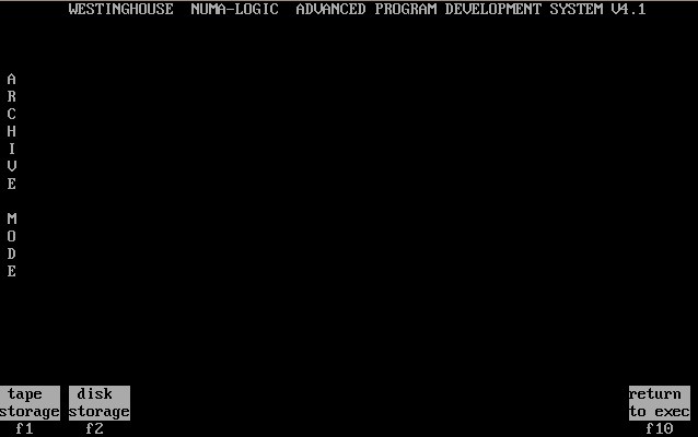
Because some of these sizes were larger than what was possible to use offline, it is necessary when working on programs with more than 32 analog inputs + 32 analog outputs and more than 8K of program to only edit these programs when connected directly to such a programmable controller. This shouldn't be a problem since most actual programs were smaller than these limits, but it is important to understand these restrictions. - Now that the system is configured for offline operation, press the F3 key on your keyboard (archive) to switch to the mode that allows storing and restored controller programs to/from disk.
- Select F2 disk storage.
- Select whether you wish to copy a program to or from disk.
Record: PLC -> Disk (F3 - Load)
Load: Disk -> PLC (F1 - Record)
Press enter after selecting.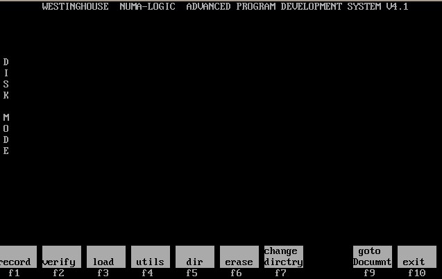
Verify compares the two and alerts if there are errors.
F4 - Utils: View directory, erase files or change directory
F5 - Dir: Allows displaying various disk directories
F6 - Erase: Allows erasing a file on any directory (or the default directory)
F7 - Change Directory: Self explanatory
F9 - Go to Document: Allows switching on documentation features (giving I/O and logic rungs specific names that are cross-referenced to the internal memory name)
Note:
When recording memory to the disk, the system will ask if you wish to store all memory or only the highest holding register referenced within your code. The reason it asks is that while you may not have an absolute reference to a register above a certain value documented within your code you may be using indirect addressing to read or write memory at any arbitrary location within the processor.
If in doubt, chose F2 - All registers, then press enter.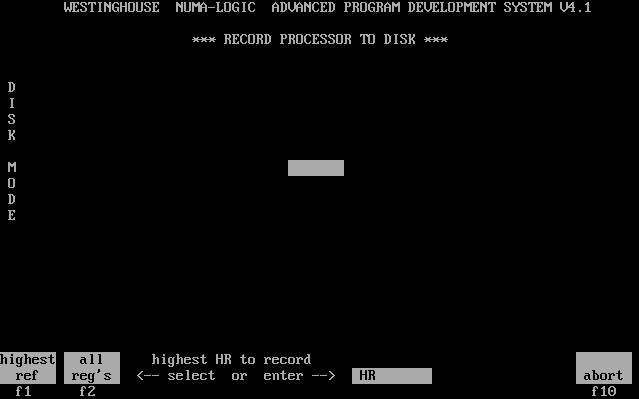
Once finished pressed the <backspace> key and you are presented with a verify menu.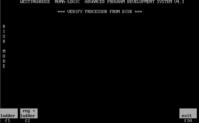
Select F2 - Registers and Ladder if you were able to select an offline processor that exactly matched your actual in-the-field processor. If not, select F1- Ladder (you'll get an error message about holding register boundaries not matching, but continue anyway).
Press <backspace> to return to the disk archive menu, or press <Esc> to return to the main menu.
#55
INCOM / IMPACC / IQ Multipoint Energy Submeter
Last post by Dave Loucks - December 26, 2014, 11:30:52 AMDue to a trademark infringment issue, the Westinghouse / Cutler-Hammer / Eaton IQ Energy Sentry II was renamed the IQ Multipoint Energy Submeter II (IQMES II). If you are looking for protocol information for the IQ MES II, be sure and also search for old literature still scattered around that use the obsolete Energy Sentry name.
For example, INCOM protocol information for the IQ MES II can be found starting on page 233 in the IMPACC Protocol Guide (Instruction Leaflet 17384): http://www.eaton.com/ecm/groups/public/@pub/@electrical/documents/content/il17384b.pdf#page=233
For example, INCOM protocol information for the IQ MES II can be found starting on page 233 in the IMPACC Protocol Guide (Instruction Leaflet 17384): http://www.eaton.com/ecm/groups/public/@pub/@electrical/documents/content/il17384b.pdf#page=233
#56
Modbus / Modbus Protocol
Last post by Dave Loucks - October 27, 2014, 11:03:46 AMI wouldn't think I would need to post a link describing the Modbus protocol here, but as I've searched the web looking for complete information, I reviewed many "page 1" hits from all manner of sites that never measured up.
So in the interest of providing readers of this site with what I consider the most complete Modbus RTU information, I am posting the link to the Modbus RTU protocol standard from Modbus.org:
Modbus Function Code 03 (Read Registers)
Note: The first byte of any Modbus request or response is always the Modbus address of the device. Likewise, the last two bytes of any Modbus request or response is always the CRC (low byte first, then high byte). That means when looking at these tables, mentally always add one extra byte to the beginning (address) and two at the end (CRC).
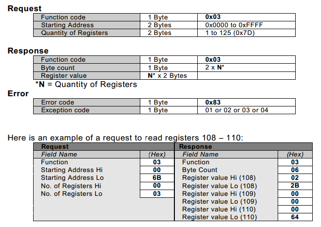
All Modbus read register (03) messages are 8 bytes long (5 shown above + 1 byte for Modbus network address + 2 CRC bytes). The acknowledgement reply response to a Modbus function code 03 message contains either 5 + (2*N) bytes for valid response or 5 bytes for exception (error) response.
mMINT Modbus Exception Codes Returned:
There are other exception codes, but these are the most common. For an example of an exception code, refer to the following exception response.
Example Exception Response (Read request of invalid block of registers)
Modbus Function Code 16 decimal (10 hex) (Write Registers)
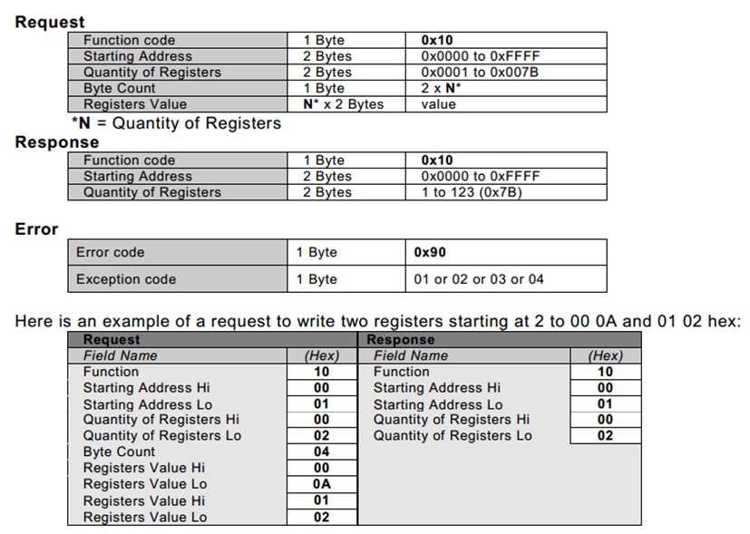
All Modbus write register (16) messages are 9 + 2*(# registers) long. The acknowledgement reply response to a Modbus function code 16 message contains either 8 bytes for valid response or 5 bytes for exception (error) response.
Another interesting note: Modbus register addressing and table lengths both are 16-bit values, therefore these 16-bit values must be divided into two bytes to transmit as a Modbus message (typical serial port settings are 8 data bits per character). The Modbus standard choses to send the high order byte first for these register addresses and table lengths.
HOWEVER, the Modbus standard states that the 16-bit CRC must be sent with the lower 8-bit byte sent first.
Example - Read two Modbus registers starting at register 46235 from Modbus address 001
Recall that Modbus registers begin with 40001 (there is no such thing as register 40000), which means if the first value has 0 offset, then the 6235th value has an offset of 6234 (one less).
Therefore, to calculate the actual address of 46235:
Sent:
Reply:
The data returned was:
Another example:
Read two registers starting with 42001:
Sent:
Reply:
The data returned was:
Writing a block of registers to a Modbus device uses Modbus function code 16 (10 hex). Modbus also supports a single register write command (06 - Preset Single Register), but the Eaton mMINT and MPONI do not support this function code.
Modbus Function Code 16 / 10 hex (Write Registers)
Sent:
As shown the Modbus read example above, the register numbers must be converted to the register addresses.
Convert 42001:
Reply:
So in the interest of providing readers of this site with what I consider the most complete Modbus RTU information, I am posting the link to the Modbus RTU protocol standard from Modbus.org:
- Modbus RTU Protocol (link points to Modbus.org)
Modbus Function Code 03 (Read Registers)
Note: The first byte of any Modbus request or response is always the Modbus address of the device. Likewise, the last two bytes of any Modbus request or response is always the CRC (low byte first, then high byte). That means when looking at these tables, mentally always add one extra byte to the beginning (address) and two at the end (CRC).
All Modbus read register (03) messages are 8 bytes long (5 shown above + 1 byte for Modbus network address + 2 CRC bytes). The acknowledgement reply response to a Modbus function code 03 message contains either 5 + (2*N) bytes for valid response or 5 bytes for exception (error) response.
mMINT Modbus Exception Codes Returned:
- 1 - Illegal Function
You used a Modbus function code that was not supported by the mMINT.
- 2 - Illegal Address
You attempted to read or write a address in the mMINT register map that does not exist (or is otherwise protected) in the device.
- 3 - Illegal Data Value
You created a message that had an invalid value in the message (such as invalid message length). Note that Modbus doesn't care what is in the data payload. This exception response is saying the construction of your messages is faulty.
- 4 - Failure in Associated Device
Message received by mMINT and validated, but no response heard from the connected device on the INCOM network.
- 5 - ACK Code
Undefined error. Solution: Repeat request. If issue remains, contact Eaton.
- 7 - mMINT Unable to Process Request
Undefined error. Solution: Repeat request. If issue remains, contact Eaton.
- 84 - Partial Table Request Error
The register address requested is valid, but you didn't request the entire 32 or 64 bit register(s). You either didn't request enough 16-bit Modbus registers, or you requested enough registers, but didn't request starting at the right register boundary.
Example: Read Ia, Ib and Ic
Ia is contained in registers 404611 and 404612, Ib is 404613/404614, Ic is 404615/404616. Assume that the programmer forgot that these are Modbus registers, not memory addresses in the Modbus message and requested address 4611 - 4616. These are valid registers, but they don't begin on the boundary of a register. You would receive an 84 exception. The correct addresses would be 4610 - 4615.
There are other exception codes, but these are the most common. For an example of an exception code, refer to the following exception response.
Example Exception Response (Read request of invalid block of registers)
| Byte | Value | Description |
| 1 | 247 | Modbus Device Address |
| 2 | 131 | Opcode (03) with 8th bit set i.e. 128+3=131 |
| 3 | 2 | Modbus Exception Code 02 (invalid address) |
| 4 | 32 | CRC - low byte |
| 5 | 195 | CRC - high byte |
Modbus Function Code 16 decimal (10 hex) (Write Registers)
All Modbus write register (16) messages are 9 + 2*(# registers) long. The acknowledgement reply response to a Modbus function code 16 message contains either 8 bytes for valid response or 5 bytes for exception (error) response.
Another interesting note: Modbus register addressing and table lengths both are 16-bit values, therefore these 16-bit values must be divided into two bytes to transmit as a Modbus message (typical serial port settings are 8 data bits per character). The Modbus standard choses to send the high order byte first for these register addresses and table lengths.
HOWEVER, the Modbus standard states that the 16-bit CRC must be sent with the lower 8-bit byte sent first.
Example - Read two Modbus registers starting at register 46235 from Modbus address 001
Recall that Modbus registers begin with 40001 (there is no such thing as register 40000), which means if the first value has 0 offset, then the 6235th value has an offset of 6234 (one less).
Modbus Register | Remove Prefix | Offset Decimal | Offset Hex |
| 40001 | 0001 | 1 | 0000 |
| 40002 | 0002 | 2 | 0001 |
| : : | : : | : : | : : |
| 46235 | 6235 | 6234 | 185A |
| : : | : : |
Therefore, to calculate the actual address of 46235:
- Remove starting 4 --> leaving 6235
- Subtract 1 --> 6234
- Convert to hexadecimal --> 185A
Sent:
- Modbus node address = 1
- Modbus function code = 3
- Modbus starting register address = 46235 (dec) (memory offset: 185A hex)
- Number of registers to read = 2
| Node | Func | Add Hi | Add Lo | # Hi | # Lo | CRC Lo | CRC Hi | |||||||
| 01 | 03 | 18 | 5A | 00 | 02 | E2 | B8 |
Reply:
Node | Func | Bytes | Data 1 Hi byte | Data 1 Lo byte | Data 2 Hi byte | Data 2 Lo byte | CRC Lo | CRC Hi | |||||||
| 01 | 03 | 04 | 04 | 88 | 00 | 00 | 7B | 29 |
The data returned was:
- 46235 = 0488 hex
- 46236 = 0000
Another example:
Read two registers starting with 42001:
- Remove starting 4 --> leaving 2001
- Subtract 1 --> 2000
- Convert to hexadecimal --> 07D0
Sent:
- Modbus node address = 247
- Modbus function code = 3
- Modbus starting register address = 42001(dec) (memory offset: 07D0 hex)
- Number of registers to read = 2
| Node | Func | Add Hi | Add Lo | # Hi | # Lo | CRC Lo | CRC Hi | |||||||
| F7 | 03 | 07 | D0 | 00 | 02 | 93 | 33 |
Reply:
Node | Func | Bytes | Data 1 Hi byte | Data 1 Lo byte | Data 2 Hi byte | Data 2 Lo byte | CRC Lo | CRC Hi | |||||||
| F7 | 03 | 04 | FF | FF | FF | FF | 6D | A8 |
The data returned was:
- 42001 = FFFF hex
- 42002 = FFFF hex
Writing a block of registers to a Modbus device uses Modbus function code 16 (10 hex). Modbus also supports a single register write command (06 - Preset Single Register), but the Eaton mMINT and MPONI do not support this function code.
Modbus Function Code 16 / 10 hex (Write Registers)
Sent:
- Modbus node address = 247
- Modbus function code = 16 decimal
- Modbus starting register address = 42001(dec) (memory offset: 07D0 hex)
- Number of registers to write = 1
- Value to write = 0
As shown the Modbus read example above, the register numbers must be converted to the register addresses.
Convert 42001:
- Remove starting 4 --> leaving 2001
- Subtract 1 --> 2000
- Convert to hexadecimal --> 07D0
| Node | Func | Add Hi | Add Lo | # Hi | # Lo | # Bytes | Data Hi | Data Lo | CRC Lo | CRC Hi | ||||||||||
| F7 | 10 | 07 | D0 | 00 | 01 | 02 | 00 | 00 | EC | A4 |
Reply:
Node | Func | Addr Hi byte | Addr Lo byte | # Regs Hi byte | # Regs Lo byte | CRC Lo | CRC Hi | |||||||
| F7 | 10 | 07 | D0 | 00 | 01 | 15 | D2 |
#57
Modbus / 2, 3 or 4-wire Modbus
Last post by Dave Loucks - October 09, 2014, 04:41:57 PMHere's a discussion of the issues around the number of wires to use in a Modbus connection. Note that at a minimum 3-wires are needed.
See http://pps2.com/smf/index.php/topic,30.0.html
See http://pps2.com/smf/index.php/topic,30.0.html
#58
Modbus / 2-wire vs. 3-wire vs. 4-wire M...
Last post by Dave Loucks - October 09, 2014, 04:39:11 PMDon't forget that most Modbus devices are 2-wire half duplex, but that they need a 3-wire connection!
Why is that?
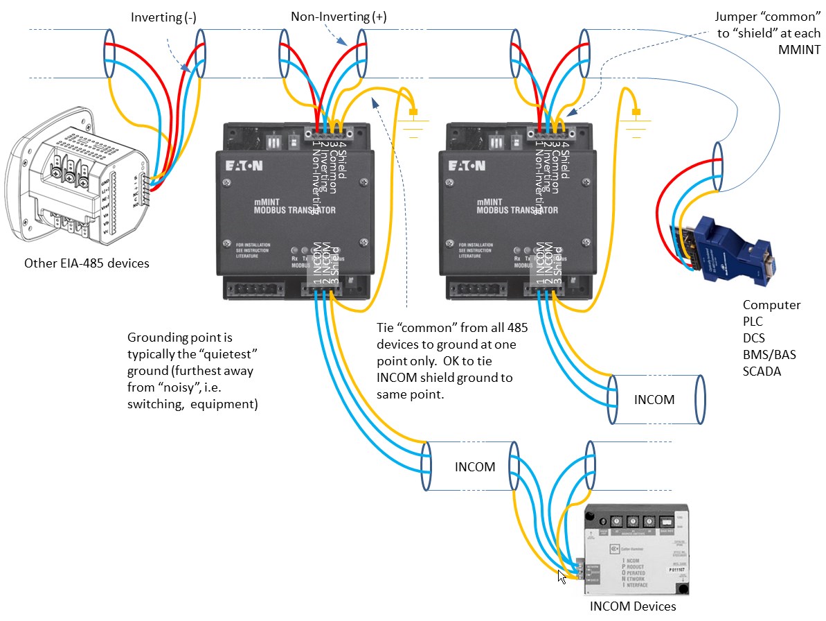
Consider an EIA-485 system with only two wires connecting the nodes together. The node transmitting places a voltage on the, for example, non-inverting wire. The diagram below is simplified (485 is a bipolar output voltage, therefore four transistors in an H-bridge are needed for each line. Here only one on each is shown).
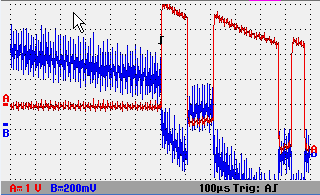
For current to flow, a complete circuit must exist from the point the voltage is placed on the non-inverting line, until it returns to the node placing the voltage on the line.

In actual systems, there will be a return path through the biasing resistors (if connected), but typical wave traces show offsets to ground over time. This can be due to line-to-ground capacitances charging and discharging.
A better system will include the 3rd (common) wire.
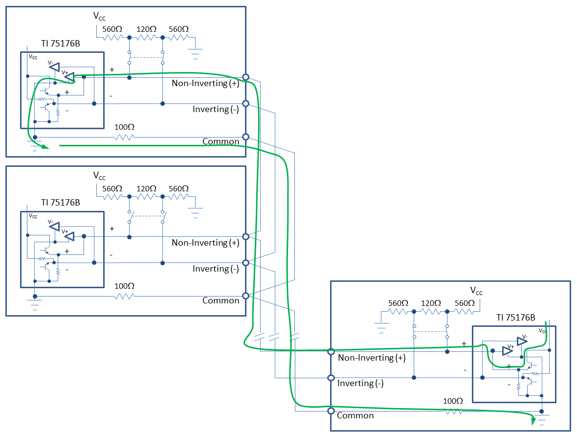
What if you only have a single twisted pair? It is acceptable to use the shield as the common. Just remember to only ground the shield at one location, but to connect the shield to the common at every device. An example is shown below:
Why is that?
Consider an EIA-485 system with only two wires connecting the nodes together. The node transmitting places a voltage on the, for example, non-inverting wire. The diagram below is simplified (485 is a bipolar output voltage, therefore four transistors in an H-bridge are needed for each line. Here only one on each is shown).
For current to flow, a complete circuit must exist from the point the voltage is placed on the non-inverting line, until it returns to the node placing the voltage on the line.
In actual systems, there will be a return path through the biasing resistors (if connected), but typical wave traces show offsets to ground over time. This can be due to line-to-ground capacitances charging and discharging.
A better system will include the 3rd (common) wire.
What if you only have a single twisted pair? It is acceptable to use the shield as the common. Just remember to only ground the shield at one location, but to connect the shield to the common at every device. An example is shown below:
#59
Modbus / Re: Modbus MINT (Modular INCOM...
Last post by Dave Loucks - September 19, 2014, 02:57:43 PMThe mMINT has a unique workaround for the problem when trying to use the Modbus RTU protocol on a network with separate "layers".
Normally, Modbus MINT addressing is just one for one - whatever Modbus address you send down the wire will be converted to the same INCOM address. The expectation, therefore, is that you cannot reuse INCOM addresses on the same Modbus network:
Very straight forward!
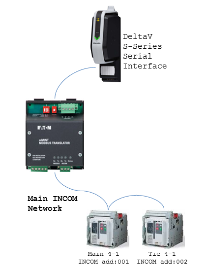
But now consider an INCOM system that uses subnetwork masters (like the Breaker Interface Module II (BIM II)):
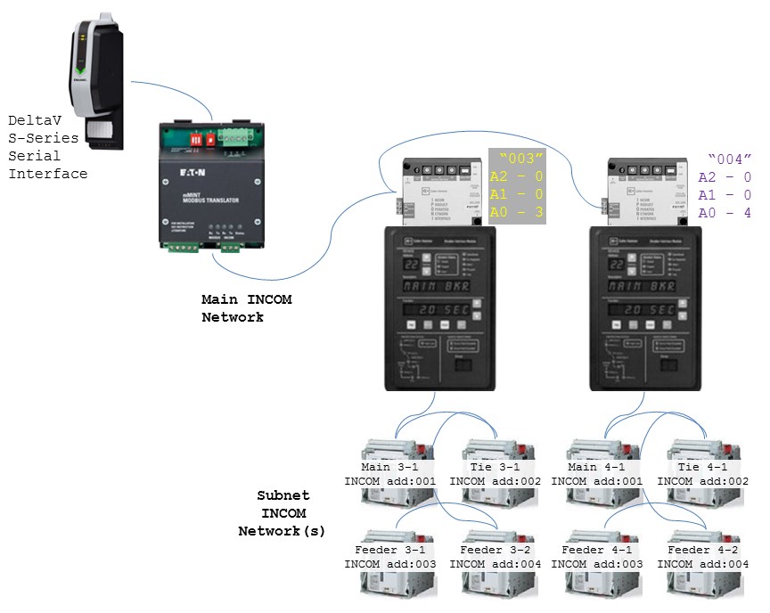
You quickly see the problem. Several of the circuit breakers have the same INCOM addresses! For example, the Main 4-1 and the Main 3-1 breakers are both addressed 001. However, since they are on different, isolated subnetworks, they don't interfere with each other. So then how does a Modbus device (like the DeltaV DCS in this example) access the correct Main breaker?
The solution is to create a routing table within the mMINT. Refer to INCOM routing address configurations found on page 6 of the mMINT - Modbus Translator Module - Instruction Leaflet IL66A7508H08 for more information.
The key is to assign each Modbus address to two separate INCOM addresses. A table of registers is set aside within the mMINT to hold this cross reference.
In the table shown immediately below, notice that Modbus address 001 is assigned two registers within the mMINT, 42101 and 42102.
The first of the two registers, 42101, holds the INCOM address of the subnet master and the second register, 42102, holds the INCOM address of the device itself.
The mMINT now knows how to route a message addressed to Modbus address 001 to the device defined by the two register pair:
A more complete routing table showing all the possible 246 (1-246) Modbus routing addresses is shown below:
Routing Table
Note: in a mixed system with both directly addressed and routed INCOM addresses, just place the value 255 (or 65535) in the routing table for the Modbus addresses and the mMINT will just use the Modbus address-to-INCOM address one-to-one mapping.
Download the attached Excel MINT_routing_template.xls spreadsheet to simplify filling in the Modbus to routing register cross-reference table. Optionally, you can use the Excel programming tool to configure these registers. The use of this tool is described in this tutorial video.
We now have enough information to know what to put in those tables. To fix the problem described above, we must enter both the circuit breaker address and the address of the subnet master (BIM II):
So even though the INCOM addresses for both breakers are the same (001), since they are on different subnetworks, the mMINT knows where to find them by using the routing table to "route" the message through the upstream BIM II's at either INCOM address 003 or 004.
Tips to Remember
(Note: a specially programmed Excel worksheet that can talk to the mMINT and perform these routing settings is available in this article further down this page.)
Here's a larger example to show how the addresses can be allocated:
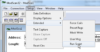
ModScan is a common tool used to send and receive Modbus messages. To send this routing table via ModScan, you will need to create a script (or manually enter a "user message").
ModScan does permit changing registers by double-clicking on the screen, but it uses Modbus function code 06, Preset Single Register, by default, which the mMINT does not support. To use the function code 16, Preset Multiple Registers, either a script must be created or, for single register writes, you can change the default behavior of Modscan to use function code 16 instead. Since you MUST change the routing table two registers at a time (subnet master and device address must both be changed at the same time -- never individually), you can't use the double-click method even if you change Modscan to use function code 16) since it will only change a single register.
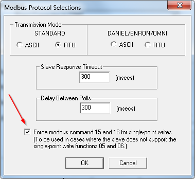
Remember, this only works for editing a single 16-bit Modbus register value. When the mMINT requires that blocks of registers be changed at once (like the subnet routing table), then use a script instead.
Modscan defines scripts on page 41 in their manual (dated 1998), but there are some tricks that are not immediately evident. One of the most important when writing data to the mMINT is the proper ordering of the values you wish to write within the script.
For example, to write the following table of registers (mMINT Subnet Routing Table), use the Modscan script immediately after this table:
Modscan Scripts
Modscan test scripts consist of ASCII text data field separated by commas. They may be constructed using any word processor or spreadsheet application (but make sure that word processor saves the file as a text file with no added characters. If you aren't sure, on a Windows computer use the NotePad application. In Excel, save your files as a comma separated variable .csv file). A test script entry consists of at least 7 data fields as depicted in the example script, (see WriteRoutingTable2.csv attached below).
When writing data, Modscan uses a unique method of requiring that 32 bits (two 16-bit registers) be written as one message.
Recommend using NotePad or other text editor, NOT Excel as Excel may try to add quotations around the '//' character pair (which won't work when imported into Modscan).
To delete a value in the routing table, simply write 0xFFFF in each register.
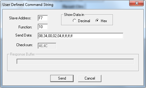
For example, assume that we wish to remove Modbus address 001 from the routing table (a message received by the mMINT, then, will be translated directly to talk to INCOM address 001 without any routing). We know that mMINT Modbus registers 42101 and 42012 control the subnet master and device addresses, respectively for Modbus address 001. Assume they presently contain routing information where 42101 contains 0001 and 42102 contains 0001. From the Modscan screen it would appear as:

To change these values to FFFF and FFFF, use the "User Msg" function in Modscan.
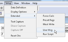
Enter the slave address of 247 or 248 (F7 or F8 hexadecimal), then the Modbus function code as 16 (10 hex).
If you are not familiar with the Modbus structure, the next part is to build the proper Modbus data string using structure of STARTING REGISTER ADDRESS, LENGTH, DATA.
We are intending to write data starting at register 2101 (Modbus prefaces holding registers with the number '4', but this isn't sent down the network) so this must be converted into a binary address to send down the wire. To represent the decimal number 2101 as a binary number (for sending down the wire), we see that 2101 decimal is 1000 0011 0101 binary, or 835 hex (use a calculator online). We are not done though -- Register numbers in Modbus always start with 1. There is no such thing as Modbus register 0. But in memory addressing, there is an address 0. The authors of Modbus stipulated that to determine the actual memory address, take the register address and subtract 1.
In this example, register number 835 hex becomes memory offset 834 hex. That second number is what we transmit down the wire. Below, the same user defined command string is formatted -- one showing values in hexadecimal and one in decimal. Notice that STARTING REGISTER = 08 34, LENGTH is 00 02 (first two numbers are the number of registers being sent) then 04 (the third number is the number of bytes... this is duplicate data since you've already inserted the number of registers and since each register is 16 bits [2 x 8-bit bytes long], then the number of bytes is known already as two times the length ... So why include both? Perhaps the inventors of Modbus used this redundancy as a form of error checking?). DATA is FF FF FF FF. Since each digit represents 4 bits and two 16-bit registers are being sent, we need 8 total hex digits. Each register is 16 bits or 4 hex digits (FFFF).

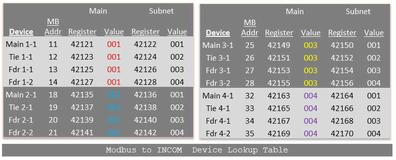
Normally, Modbus MINT addressing is just one for one - whatever Modbus address you send down the wire will be converted to the same INCOM address. The expectation, therefore, is that you cannot reuse INCOM addresses on the same Modbus network:
| Modbus Address | INCOM Address | |
| Main 4-1 | 001 | 001 |
| Tie 4-1 | 002 | 002 |
Very straight forward!
But now consider an INCOM system that uses subnetwork masters (like the Breaker Interface Module II (BIM II)):
You quickly see the problem. Several of the circuit breakers have the same INCOM addresses! For example, the Main 4-1 and the Main 3-1 breakers are both addressed 001. However, since they are on different, isolated subnetworks, they don't interfere with each other. So then how does a Modbus device (like the DeltaV DCS in this example) access the correct Main breaker?
The solution is to create a routing table within the mMINT. Refer to INCOM routing address configurations found on page 6 of the mMINT - Modbus Translator Module - Instruction Leaflet IL66A7508H08 for more information.
The key is to assign each Modbus address to two separate INCOM addresses. A table of registers is set aside within the mMINT to hold this cross reference.
In the table shown immediately below, notice that Modbus address 001 is assigned two registers within the mMINT, 42101 and 42102.
The first of the two registers, 42101, holds the INCOM address of the subnet master and the second register, 42102, holds the INCOM address of the device itself.
The mMINT now knows how to route a message addressed to Modbus address 001 to the device defined by the two register pair:
| Modbus Address | Subnet Master Stored Here | Device Address Stored Here | ||
001 | 42101 | 42102 |
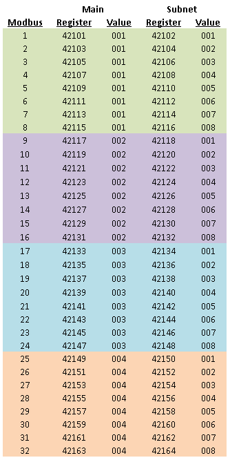
A more complete routing table showing all the possible 246 (1-246) Modbus routing addresses is shown below:
Routing Table
Modbus Address | INCOM Main Network Address | INCOM Sub- NetworkAddress |
001 | 42101 | 42102 |
002 | 42103 | 42104 |
: : | : : | : : |
246 | 42591 | 42592 |
Note: in a mixed system with both directly addressed and routed INCOM addresses, just place the value 255 (or 65535) in the routing table for the Modbus addresses and the mMINT will just use the Modbus address-to-INCOM address one-to-one mapping.
Download the attached Excel MINT_routing_template.xls spreadsheet to simplify filling in the Modbus to routing register cross-reference table. Optionally, you can use the Excel programming tool to configure these registers. The use of this tool is described in this tutorial video.
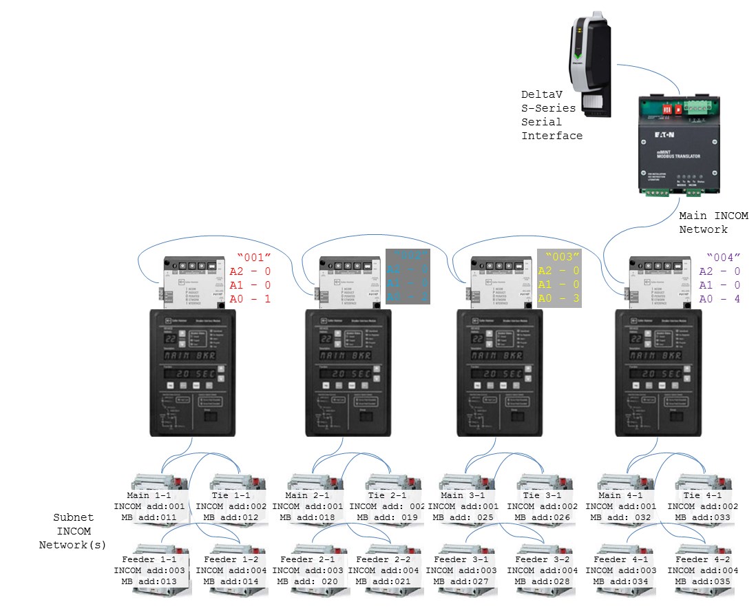
We now have enough information to know what to put in those tables. To fix the problem described above, we must enter both the circuit breaker address and the address of the subnet master (BIM II):
Modbus Address | Points to: | INCOM Main Network Address | INCOM Sub- NetworkAddress |
001 | Main 3-1 | 42101=003 | 42102=001 |
002 | Main 4-1 | 42103=004 | 42104=001 |
So even though the INCOM addresses for both breakers are the same (001), since they are on different subnetworks, the mMINT knows where to find them by using the routing table to "route" the message through the upstream BIM II's at either INCOM address 003 or 004.
Tips to Remember
(Note: a specially programmed Excel worksheet that can talk to the mMINT and perform these routing settings is available in this article further down this page.)
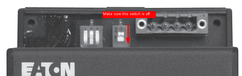
- The mMINT is a pass-through device. To read or write any Modbus registers on the mMINT device itself, remember you must give the mMINT its own Modbus network address. To do so, move DIP SW2-1 to the OPEN position:
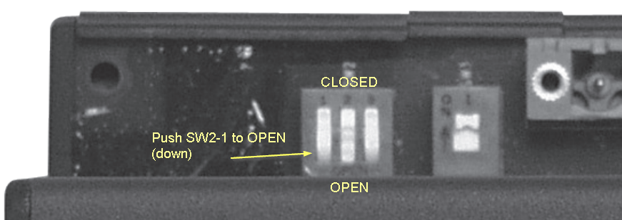
The mMINT's Modbus address is then set to 247 (248 also works).
NOTE: the position of DIP switch 2 may be rotated 180 degrees (upside down) from what is shown on this picture (in other words, OPEN would be away from the mMINT housing). Be sure to look closely at the switch for the printed words OPEN (or CLOSED) and set switch OPEN to activate the Modbus addresses 247 and 248.
NOTE: The mMINT originally could only be addressed using Modbus node 248. In V1.06 firmware a change was made that when SW2-1 was opened BOTH addresses 248 AND 247 would be activated. This change was made because some Modbus masters could not access a slave device above 247. A complete list (CodeRevisions.txt) of all mMINT firmware revisions is attached immediately below this subarticle.
- Using Modscan or other Modbus master program, send Modbus function code 1610 (1016) [Write Multiple Registers] to address 247 or 248 (either one works) along with the data in registers 42101 to ... (where the last register is dependent on how many look up entries you wish to use. An Excel spreadsheet is attached that shows the cross-reference between Modbus addresses and the lookup register pair stored within the mMINT.
- Move SW2-1 back to the CLOSED position once you are done. (You can technically keep the switch in the OPEN position, but doing so keeps the ability to make remote changes to its flash configuration which might be a security issue. Also, having two or more mMINTs with SW2-1 open would place two more more devices with address 247 and 248 on the same network. Collisions will result. On the other hand, note that moving SW2-1 back to closed not only locks out the ability to make remote changes, but it also prevents viewing mMINT diagnostic registers on that mMINT. For this reason, it may make sense to place each mMINT on its own Modbus network.)
Here's a larger example to show how the addresses can be allocated:
ModScan is a common tool used to send and receive Modbus messages. To send this routing table via ModScan, you will need to create a script (or manually enter a "user message").
| Running a Script | Entering a Message Manually | |
 | |
ModScan does permit changing registers by double-clicking on the screen, but it uses Modbus function code 06, Preset Single Register, by default, which the mMINT does not support. To use the function code 16, Preset Multiple Registers, either a script must be created or, for single register writes, you can change the default behavior of Modscan to use function code 16 instead. Since you MUST change the routing table two registers at a time (subnet master and device address must both be changed at the same time -- never individually), you can't use the double-click method even if you change Modscan to use function code 16) since it will only change a single register.
Remember, this only works for editing a single 16-bit Modbus register value. When the mMINT requires that blocks of registers be changed at once (like the subnet routing table), then use a script instead.
Modscan defines scripts on page 41 in their manual (dated 1998), but there are some tricks that are not immediately evident. One of the most important when writing data to the mMINT is the proper ordering of the values you wish to write within the script.
For example, to write the following table of registers (mMINT Subnet Routing Table), use the Modscan script immediately after this table:
Modscan Scripts
Modscan test scripts consist of ASCII text data field separated by commas. They may be constructed using any word processor or spreadsheet application (but make sure that word processor saves the file as a text file with no added characters. If you aren't sure, on a Windows computer use the NotePad application. In Excel, save your files as a comma separated variable .csv file). A test script entry consists of at least 7 data fields as depicted in the example script, (see WriteRoutingTable2.csv attached below).
When writing data, Modscan uses a unique method of requiring that 32 bits (two 16-bit registers) be written as one message.
Recommend using NotePad or other text editor, NOT Excel as Excel may try to add quotations around the '//' character pair (which won't work when imported into Modscan).
Code Select
//
// Modbus Test Script for ModScan Application
//
// Each Script entry consists of the following comma delimited data fields:
// TEST NAME, NODE, FUNCTION, ADDRESS, LENGTH, DATA, CONTROL CODE
//
// Double slashes on the front of a line denote comments
//
// The following Control Codes may be used (i.e. last field on each line)
//					\ -- Continue DATA fields on next line"
//					C -- Generate Bad CRC message to slave"
//					D -- Check response data quantity only", (ignore actual data)
//					1 -- Expect Exception Response 01"
//					2 -- Expect Exception Response 02"
//					4 -- Expect Exception Response 04"
//					R -- Expect no Response"
//					T (default) -- Verify Response Data"
//
//
//          -----------------------------------------------
//          mMINT diagnostics communications (SW2-1 ""OPEN"")"
//          -----------------------------------------------
//
// mMINT Echo Test:
//   Echo Test (Diagnostic Function 08  SubFunction 0x0000)
//   TEST NAME, NODE, FUNCTION, SUBFUNCTION, LENGTH, DATA, CONTROL CODE
E1. mMINT Echo Test,248,8,0x0000,1,0xAA55,T
//
//   Config Block (Preset Multiple Registers 0x10  Address 2100)
//   TEST NAME, NODE, FUNCTION, ADDRESS, NBR REGS,Data
1A. Config Map 0-1,248,16,2101,64,\
,0x00010001,0x00020001,0x00030001,0x00040001,0x00050001,0x00060001,0x00070001,0x00080001,\
,0x00010002,0x00020002,0x00030002,0x00040002,0x00050002,0x00060002,0x00070002,0x00080002,\
,0x00010003,0x00020003,0x00030003,0x00040003,0x00050003,0x00060003,0x00070003,0x00080003,\
,0x00010004,0x00020004,0x00030004,0x00040004,0x00050004,0x00060004,0x00070004,0x00080004,\
T
// This message will send out the following data:
//N  - Modbus node address
//fn - Modbus function code
//add- Starting register address - 1 (e.g. 42101 dec = 0835 hex subtract 1 = 0834 address)
//num- Number of registers to write
//by - Bytes sent (redundant to num, but Modbus uses as a form of error checking)
// 1 - Hi byte, Lo byte of first register value
// 2 - Hi byte, Lo byte of second register value
// :	:	:	:
//64 - Hi byte, Lo byte of 64th register value
//
//N  fn  add   num  by   1     2     3     4     5     6     7     8     9    10
//F8,10,08,34,00,40,80,00,01,00,01,00,01,00,02,00,01,00,03,00,01,00,04,00,01,00,05,
// 11    12    13    14    15    16    17    18    19    20    21    22    23
//00,01,00,06,00,01,00,07,00,01,00,08,00,02,00,01,00,02,00,02,00,02,00,03,00,02,
// 24    25    26    27    28    29    30    31    32    33    34    35    36    37
//00,04,00,02,00,05,00,02,00,06,00,02,00,07,00,02,00,08,00,03,00,01,00,03,00,02,00,03,
// 38    39    40    41    42    43    44    45    46    47    48    49    50
//00,03,00,03,00,04,00,03,00,05,00,03,00,06,00,03,00,07,00,03,00,08,00,04,00,01,
//  51   52    53    54    55    56    57    58    59    60    61    62    63    64
//00,04,00,02,00,04,00,03,00,04,00,04,00,04,00,05,00,04,00,06,00,04,00,07,00,04,00,08,
//CL CH
//76,49
//
//
// END OF SCRIPT
end
To delete a value in the routing table, simply write 0xFFFF in each register.
For example, assume that we wish to remove Modbus address 001 from the routing table (a message received by the mMINT, then, will be translated directly to talk to INCOM address 001 without any routing). We know that mMINT Modbus registers 42101 and 42012 control the subnet master and device addresses, respectively for Modbus address 001. Assume they presently contain routing information where 42101 contains 0001 and 42102 contains 0001. From the Modscan screen it would appear as:
To change these values to FFFF and FFFF, use the "User Msg" function in Modscan.
Enter the slave address of 247 or 248 (F7 or F8 hexadecimal), then the Modbus function code as 16 (10 hex).
If you are not familiar with the Modbus structure, the next part is to build the proper Modbus data string using structure of STARTING REGISTER ADDRESS, LENGTH, DATA.
We are intending to write data starting at register 2101 (Modbus prefaces holding registers with the number '4', but this isn't sent down the network) so this must be converted into a binary address to send down the wire. To represent the decimal number 2101 as a binary number (for sending down the wire), we see that 2101 decimal is 1000 0011 0101 binary, or 835 hex (use a calculator online). We are not done though -- Register numbers in Modbus always start with 1. There is no such thing as Modbus register 0. But in memory addressing, there is an address 0. The authors of Modbus stipulated that to determine the actual memory address, take the register address and subtract 1.
In this example, register number 835 hex becomes memory offset 834 hex. That second number is what we transmit down the wire. Below, the same user defined command string is formatted -- one showing values in hexadecimal and one in decimal. Notice that STARTING REGISTER = 08 34, LENGTH is 00 02 (first two numbers are the number of registers being sent) then 04 (the third number is the number of bytes... this is duplicate data since you've already inserted the number of registers and since each register is 16 bits [2 x 8-bit bytes long], then the number of bytes is known already as two times the length ... So why include both? Perhaps the inventors of Modbus used this redundancy as a form of error checking?). DATA is FF FF FF FF. Since each digit represents 4 bits and two 16-bit registers are being sent, we need 8 total hex digits. Each register is 16 bits or 4 hex digits (FFFF).
#60
Modbus / Modbus MINT (Modular INCOM Net...
Last post by Dave Loucks - September 12, 2014, 11:30:51 AMThe mMINT is used to connect devices that use the INCOM protocol to a Modbus RTU network via a 485 twisted pair network.

A more complex diagram could look like this:
When using computers with USB ports connected to 485 converters, take care to identify the "inverting" from the "non-inverting" terminals on each device. Always connected like terminals (inverting to inverting, non-inverting to non-inverting). Do not look at letters (A or B, for example) as different vendors ascribe different meanings to those letters).
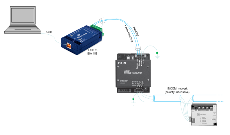
The Modbus MINT (mMINT) allows a Modbus master device to collect data from INCOM slave devices. The mMINT supports two methods of collecting data.
Preset Modbus Register Map
Refer to Tables 8 and 9 in the Modbus MINT instruction manual.
Some important notes:
Custom Pass-Through
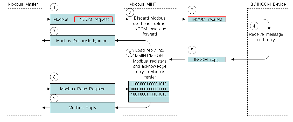
If the data you desire from the downstream INCOM device is not stored within the mMINT Modbus register map, you can send what is called a "pass-through" message using the Modbus protocol that the mMINT will interpret as special instructions to fetch data from an INCOM device. That process requires two (or more) Modbus messages and is graphically shown below.
Besides the instruction manual that you can download from the Eaton web site, I also wrote a few other app notes that might help.
Troubleshooting:
Following the instructions in the Modbus MINT Application document attached, but some key things to watch:
No response?
Invalid Responses
A more complex diagram could look like this:
When using computers with USB ports connected to 485 converters, take care to identify the "inverting" from the "non-inverting" terminals on each device. Always connected like terminals (inverting to inverting, non-inverting to non-inverting). Do not look at letters (A or B, for example) as different vendors ascribe different meanings to those letters).
The Modbus MINT (mMINT) allows a Modbus master device to collect data from INCOM slave devices. The mMINT supports two methods of collecting data.
- Preset Modbus Register Map
- Custom Pass-Through
Preset Modbus Register Map
Refer to Tables 8 and 9 in the Modbus MINT instruction manual.
Some important notes:
- The mMINT does NOT poll the INCOM devices without a request being received from the Modbus master. The mMINT does not have the data waiting in Modbus registers from the INCOM devices.
- When a command supported by the mMINT is received from the Modbus master, the mMINT will send a Fast Status to see if the device is under it.
- If so it logs it in and continues to process the command (i.e., do more INCOM transfers to obtain the data).
- If the device is logged in (and would be logged back off with about 5 consecutive no responses from the INCOM device), it simply processes the command (INCOM transfers) without the FS.
- It is important to note that the mMINT response to the Modbus master is delayed waiting for the INCOM responds. The mMINT needs to obtain all the data from the INCOM network and organize it into the Modbus register format response.
- Even when the mMINT receives a command for a Modbus device address not under the mMINT, it will send the FS out on INCOM (will get a timeout and not log it in).
- Also, the initial time the mMINT needs to get an object, it will try all the various ways to get the data from INCOM and log that way for that device.
Future accesses for that object will then always use that INCOM command.
Custom Pass-Through
If the data you desire from the downstream INCOM device is not stored within the mMINT Modbus register map, you can send what is called a "pass-through" message using the Modbus protocol that the mMINT will interpret as special instructions to fetch data from an INCOM device. That process requires two (or more) Modbus messages and is graphically shown below.
Besides the instruction manual that you can download from the Eaton web site, I also wrote a few other app notes that might help.
- Modbus MINT Application (attached below)
- IQ/Digitrip Communications
- Transfer Switch Communications
Troubleshooting:
Following the instructions in the Modbus MINT Application document attached, but some key things to watch:
No response?
- Make sure downstream devices are powered up! Trip units, for example, won't respond unless sufficient current is flowing through them (or the optional auxiliary power supply is installed) because the microprocessor is not powered
- If using a subnet master on the INCOM network (like a Breaker Interface Module or BIM), make sure you have uploaded the subnetwork routing table to the mMINT. See article on Subnetwork Routing below.
- Check 485 polarity (some devices use A & B, but the meaning of A & B (is A + or -?) changes between vendors.
- Check 485 termination switch (only close if at end of line). If the mMINT is not at the end of the 485 line, make sure SW3 is OFF.
If the mMINT is a the end of a 485 line, make sure SW3 is ON.
Invalid Responses
- Check 485 termination switch (only close if at end of line).
- INCOM devices disconnecting? The mMINT will remember that an INCOM device was there so if a Modbus request arrives for that (previously available) INCOM device, the mMINT will respond with an error oinly for the first 5 attempts. After 5 attempts the mMINT will stop responding with a Modbus error message and instead go silent until the INCOM device at that address once again is restored to operation.